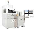
Rudolph NSX Selected For Inspection And Metrology Of New Through-Silicon Via Process

Tokyo, Japan - Rudolph Technologies, Inc., a worldwide leader in process characterization solutions for the semiconductor manufacturing industry, announced recently the successful installation of an NSX 115 Macro Inspection System at a major European fab. The NSX is being used for high-volume inspection and metrology of next-generation production processes, including through-silicon vias (TSV). The NSX will support one of the first applications of TSV manufacturing to be put into production for CMOS imaging sensors.
"Our NSX Series was evaluated along with several other inspection systems for this next-generation process," said Rajiv Roy, Rudolph's vice president of business development and director of back-end product management. "The TSV package for sensors is made up of a complex stack of materials including glass, epoxy, and of course, silicon. The NSX proved itself to be flexible enough to inspect various materials and, as such, can be used at multiple stages of the overall assembly of the TSV sensor".
According to Roy, "As evidenced by the competitive evaluation, the NSX is likely the best fit for this customer and this particular application. TSV is still an emerging application and process challenges certainly remain. But, the NSX is designed to provide an inspection and metrology solution that addresses these challenges for both process development and high-volume production—on the same platform."
The NSX Series is a fast, repeatable macro defect inspection solution used primarily for final assembly, test and packaging applications in the semiconductor device manufacturing process. Specifically designed for the back-end manufacturing environment, the NSX delivers the same sensitivity and throughput as Rudolph's front-end inspection tools without the cost burden of clean room compatibility. It handles whole wafers and thinned wafers on film frames. The NSX Series provides high-speed 2D inspection and metrology and detailed 3D characterization of filled and capped TSVs as well as other more conventional applications, including solder bumps, under-pad metallization and probe marks.
SOURCE: Rudolph Technologies
